About PCB Clone Service
PCB Clone is a professional electronic reverse engineering technology used to duplicate existing printed circuit boards with no original design files available. This technical service precisely replicates every physical and electrical feature of the original circuit board. It helps electronics engineers and enterprises recover lost PCB design data efficiently. Many electronic devices and industrial equipment lose their original manufacturing files after years of operation. Original manufacturers may stop production or discontinue technical support. Traditional maintenance methods cannot solve the problem of missing PCB documents. Our PCB cloning service provides a reliable solution for legacy hardware recovery. We adopt high-precision industrial scanning and layer analysis technology for every cloning project. Each copper trace, pad, via and wiring route is captured with microscopic accuracy. The service supports single-layer, double-layer and multi-layer PCB boards of all thicknesses. It covers ordinary rigid boards, flexible boards, rigid-flex boards and high-density HDI circuits. Professional engineers conduct layer-by-layer disassembling and scanning for multilayer PCBs. Inner layer wiring structures are completely recorded without missing any circuit details. Component distribution positions and pin definitions are fully consistent with the original sample.
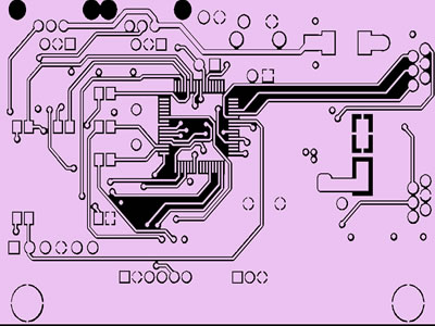
We rebuild standard Gerber files, drill files and manufacturing documents. Complete BOM lists are generated including component models, specifications and brand information. Editable schematic diagrams are restored to support circuit analysis and secondary development. PCB cloning effectively solves the problem of discontinued industrial equipment maintenance. It allows enterprises to replicate critical control boards and restore normal production operations. The service is widely used in industrial control, automotive electronics, medical devices and communication equipment. It supports small-batch duplication, prototype verification and product upgrade modification. Every cloned board maintains identical electrical performance and signal characteristics as the original. We strictly control line width, line spacing, impedance parameters and layer stack structure. All technical parameters comply with international PCB manufacturing standards. Our team eliminates manual errors through standardized scanning and software reconstruction. Each finished file undergoes multi-round comparison and verification against the original board. Customers can directly use the output files for PCB production and SMT assembly. PCB clone technology also supports circuit optimization and defect repairing based on original boards. Engineers can modify unreasonable wiring structures and improve board stability. It helps reduce production costs and enhance product market competitiveness.
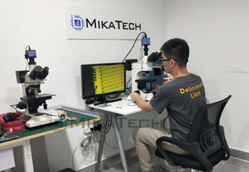
The whole process is non-destructive for single-layer and double-layer boards. Multilayer boards require professional layer separation for complete internal data acquisition. All project data is kept strictly confidential with complete privacy protection mechanisms. We provide one-stop services from board evaluation, data reconstruction to file delivery. Fast processing cycles meet urgent engineering and maintenance demands. Professional technical guidance is offered for every project throughout the process. High-resolution microscopic imaging ensures zero deviation in trace restoration. Our long-term accumulated experience supports complex high-precision board cloning. We handle high-frequency boards, thick copper boards and impedance control boards professionally. The service greatly shortens product development cycles for electronic enterprises. It avoids repeated design work and saves massive R&D costs. PCB cloning has become an essential technical support for electronic hardware innovation. It bridges the gap between physical hardware and digital design files. It provides reliable technical data for equipment upgrading, fault analysis and technical research. It helps global enterprises solve various hardware data recovery difficulties efficiently.
