Microcontroller decapsulation is a professional semiconductor physical analysis process used to remove external epoxy packaging of MCU chips. This advanced technical service aims to safely expose the internal silicon die without causing unnecessary structural damage. Every microcontroller on the market is protected by thick resin packaging to shield internal circuits from external interference. The outer packaging protects tiny die cores, metal bonding wires, internal circuit traces and security fuse modules. Ordinary disassembly methods cannot access these microscopic internal structures. Professional decapsulation technology provides effective physical access for chip research and testing. Our service covers all common microcontroller series and package forms. We support DIP, SOIC, QFP, QFN, BGA and PLCC packaged MCU devices. We adopt two mainstream technical solutions including chemical decapsulation and laser decapsulation. Each solution is carefully selected according to chip package thickness and internal structure sensitivity. Chemical decapsulation uses precise acid etching to dissolve epoxy layers evenly. Laser decapsulation utilizes high-precision laser ablation for non-contact packaging removal. Both methods can effectively retain complete bonding wires and die surfaces. Microcontroller decapsulation is the core foundation of hardware failure analysis. Many MCU failures cannot be identified through conventional electrical testing. Internal burnout, circuit breakdown and wafer defects can only be observed after decapsulation.
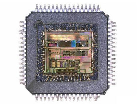
This service helps engineers locate short-circuit points and damaged circuit areas accurately. It also supports counterfeit chip detection and component authenticity verification. Many recycled and remarked MCUs hide internal aging and damage problems. Decapsulation can expose hidden physical defects and counterfeit traces clearly. The service is widely applied in embedded system reverse engineering. Researchers rely on decapsulation to observe original die layout and circuit design. It helps analyze firmware storage mechanisms and hardware security structures. Protected microcontrollers usually set physical security locks on the silicon die. Decapsulation allows technicians to observe security fuse status and encryption structures. This supports hardware security evaluation and vulnerability research. Industrial maintenance teams use decapsulation to repair discontinued MCU equipment. Many old industrial devices adopt obsolete microcontroller models without public technical documents. Decapsulation helps restore original circuit design data for equipment maintenance. The process strictly controls reaction time and working temperature to avoid die damage. Our technical team performs step-by-step residue cleaning after packaging removal. We remove excess epoxy residuals without scratching metal traces. Each decapsulated sample undergoes strict visual inspection under industrial microscopes.
We check bonding wire integrity, pad status and die surface cleanliness. Qualified samples will be photographed and recorded with high-resolution imaging. We provide complete observation data and professional analysis reports for every project. All processing procedures follow international semiconductor analysis standards. We guarantee stable success rate and low damage rate for mass samples. Our service supports single sample testing and batch engineering processing. We provide customized solutions for special ceramic packaging and ultra-thin packaging chips. Microcontroller decapsulation is a necessary technical means for semiconductor research. It bridges the gap between external electrical testing and internal physical structure analysis. It provides reliable physical evidence for product certification and failure tracing. It effectively supports enterprise product improvement and technical research and development. It also provides important technical support for university scientific research and laboratory projects. Every procedure is operated by experienced semiconductor engineers. We avoid artificial damage and excessive corrosion during processing. We ensure that the internal original state of the chip is maximally retained. Customers can obtain intuitive die images and complete structural analysis results. This service has become an essential technical support for the electronics industry. It continues to help global enterprises solve various MCU internal analysis problems efficiently.
