MCU optic microscope imaging is a key semiconductor physical inspection service focused on microcontroller visual documentation. It uses industrial optical microscopes to observe and record tiny internal chip structures. This service is usually performed after microcontroller decapsulation operations. The exposed silicon die, bond wires and contact pads become observable under optical magnification. Different magnification levels can be applied according to project requirements. Low magnification captures full‑frame overview of the whole die and package layout. Medium magnification shows bond wire routing and pad distribution status. High magnification reveals fine surface features, burn marks and microscopic defects. The imaging workflow supports both bright‑field and dark‑field illumination modes. Multi‑angle lighting helps to highlight scratches, cracks and residual epoxy traces. All captured images are saved in high‑resolution lossless picture formats. Customers receive original source files besides compressed preview copies.
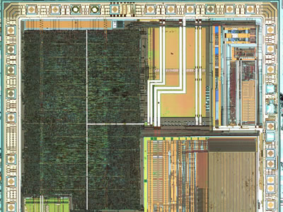
MCU optical imaging serves multiple technical research scenarios in electronics industry. Hardware reverse‑engineering teams rely on these visual records to study die layout. Failure analysis engineers locate burn spots, short‑circuit traces and physical damage. Hardware security researchers inspect security fuse bits and anti‑tamper structures. Component authentication work uses microscope photos to judge counterfeit chip signs. It can also record bonding wire offset, breakage and poor connection phenomena. The service accepts already‑decapsulated samples as well as full turn‑key solutions. Turn‑key solutions include decapsulation process plus complete optical imaging deliverables. Operators carefully adjust focus, exposure and light angle for each sample. Surface dust and residual contaminants are cleaned before formal shooting. Every area of interest is photographed repeatedly to avoid missing key details. Complete image sets are organized and labelled for easy customer review. Standard deliverables include overview shots and close‑up detail snapshots. Optional extended services include image stitching for large‑area die panorama. Image stitching combines multiple frames into one complete high‑resolution die photograph.
The service supports all mainstream MCU package types after proper sample preparation. DIP, SOIC, QFP, QFN, BGA and PLCC samples can be processed. It works for various MCU families including ARM Cortex‑M, 8051, PIC and RISC‑V chips. Optical microscope imaging is non‑destructive to already opened chip samples. No further chemical or laser damage will be introduced during shooting. The original physical sample will be returned together with digital image files. Engineers can observe bond wire integrity without risking additional physical destruction. Optical imaging often acts as the first observation step before more advanced analysis. It provides low‑cost preliminary evidence before SEM or other expensive testing. Many research projects start with optical microscope documentation for screening. Abnormal spots found in optical images guide subsequent deeper‑level analysis. Our team strictly follows semiconductor laboratory operating specifications. Each project keeps clear records of magnification parameters and lighting settings. Customers can reference these parameters when reviewing delivered material. Batch sample processing is available for engineering evaluation projects. Single‑piece sample testing is also supported for laboratory research tasks. All output materials can be used for internal reports, research documents and project archives. MCU optic microscope imaging builds a visual bridge between real silicon hardware and technical analysis work. It converts invisible tiny chip structures into usable digital visual resources for engineers worldwide.
